In the industry of printed circuit board manufacturing, you may have heard both the terms blind via and buried via. To understand the answer,Pls continue to look the below about bind and buried vias PCB.
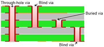
Blind and buried vias are used to connect between layers of a PCB where space is at a premium. A Blind Via connects an outer layer to one or more inner layers but does not go through the entire board. A Buried Via connects two or more inner layers but does not go through to an outer layer.

What Is a Blind Via?
Blind vias is connected from inner layer to outer layer,it does not penetrate the entire board.
What Is a Buried Via?
The buried vias is connected between inner layers, which can not be seen from the surface of PCB.
What Is a Via?Vias are the copper-plated holes in the printed circuit board that allows the layers to connect. The standard via is called a through-hole via, but there are several disadvantages to using through-hole vias in Surface Mount Technology (SMT). For this reason, we often use a blind via or buried via instead. A blind or buried via can be processed in a wide range of different measures, including plugged copper mask via, a plugged solder mask via, plated via or staggered via.
FanyPCB has many years of experience in manufacturing printed circuit boards of blind and buried vias. No matter what it happends, we can make completely blind or buried via PCB you need for your application.

