
Products & Service
 "/>
"/>Introduce
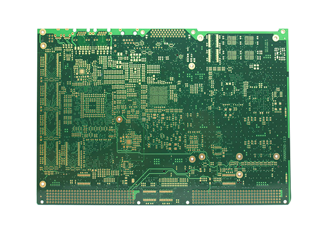
Item:14 layer blind and buried via pcb
Number of layers:14 layers
Special techinical:blind and buried vias PCB
Surface treatment:Immersion gold
Material:FR4
Outer layer line width/space:4/5mils
Inner layer line width/space:4/3.5mils
Board Thickness:1.6mm
Min. drilling hole size:0.2mm
Application:Industrial Control Mainboard
Related news
14 Layer blind and buried via pcb
Related Tags
-
multilayer PCB
Half hole PCB
Special PCB
fr4 pcb
HDI PCB
rf pcb
PCB layout design
HDI
aluminum pcb
high frequency pcb
flexible pcb
Rogers PCB
osp pcb
2 layer pcb
High TG PCB
Microwave PCB
double sided pcb
Heavy Cooper board
two layer pcb
Lead free HASL PCB
2 side pcb
PCB layout
pcb design
rigid-flex pcb
| Date | Theme |
| 2019-12-04 | Adesto and Cadence collaborate on xSPI ecosystem for IoT |
| 2019-11-05 | Teach you how to draw a simple PCB schematic in seven steps |
| 2019-11-28 | Happy Thanksgiving in FanyPCB |
| 2019-10-23 | Design rulers are the key to the success of PCB design |
| 2019-11-11 | How to make a perfect PCB layout through seven steps? |