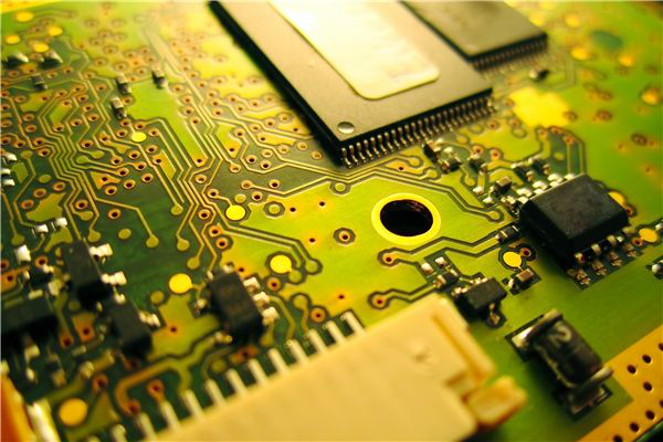
If High-speed PCB layout design can be as simple as connecting the schematic nodes and as beautiful as seen on a computer monitor, that would be a wonderful thing. Actually, High difficult PCB layout is usually not as easy as the circuit design they are working on. PCB layout design engineers face many new challenges before PCB design finally works and some people affirm performance. This is the current state of high-speed PCB layout design – layout design rules and design guidelines constantly evolving.
Most of PCB Circuit boards are the result of collaboration between schematic designers and professional layout PCB designers.The success or failure of the final circuit board is responsible for the schematic designer. Schematic PCB designers know more about excellent layout techniques to avoid major problems.
If the PCB layout design contains a high-density FPGA, there are likely to be many challenges placed in front of a well-designed schematic. Including hundreds of input and output ports, operating frequencies exceeding 500MHz (which may be higher in some designs), and solder ball pitches as small as half a millimeter, etc., all of which will cause negative effect between the design units.
So What can we do? Please contact us or send email pcb@fany-eda.com.
As the signal speeds increase, it becomes increasingly difficult to easily transfer data on circuit board. Other techniques can be utilized to further enhance.

Finally, it is also one of the best ways. Refer to the reference board provided by the FPGA manufacturer. Most manufacturers will provide source layout information for the reference board, although special requests may be required due to private information issues. These boards typically contain standard high-speed I/O interfaces that are required by FPGA manufacturers to characterize and authenticate their devices. Keep in mind, however, that these boards are often designed for a variety of uses and do not necessarily match the specific design requirements. Even so, they can still serve as a starting point for creating solutions.
The key is to figure out what the goal is before investing a lot of time and effort into PCB layout design. Once the layout is complete, redesigning will take a lot of time and money, even with a slight adjustment to the width of the trace. You can’t rely on PCB layout engineers to make PCB designs that meet your actual needs. The schematic designer must always provide guidance, make smart choices, and take responsibility for the success of the solution.

