
Products & Service
 "/>
"/>Introduce
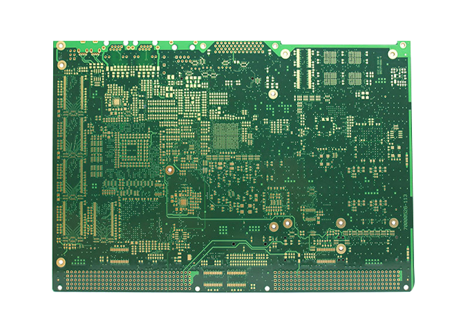
Item:14 layer blind and buried via pcb
Number of layers:14 layers
Special techinical:blind and buried vias PCB
Surface treatment:Immersion gold
Material:FR4
Outer layer line width/space:4/5mils
Inner layer line width/space:4/3.5mils
Board Thickness:1.6mm
Min. drilling hole size:0.2mm
Application:Industrial Control Mainboard
Related news
14 Layer blind and buried via pcb
Related Tags
-
PCB layout
Half hole PCB
osp pcb
rigid-flex pcb
Lead free HASL PCB
Heavy Cooper board
High TG PCB
fr4 pcb
2 layer pcb
HDI
Rogers PCB
Special PCB
Microwave PCB
multilayer PCB
two layer pcb
rf pcb
flexible pcb
double sided pcb
high frequency pcb
PCB layout design
pcb design
aluminum pcb
2 side pcb
HDI PCB