In the industry of printed circuit board manufacturing, you may have heard both the terms blind via and buried via. To understand the answer,Pls continue to look the be……
read moreTechnical News
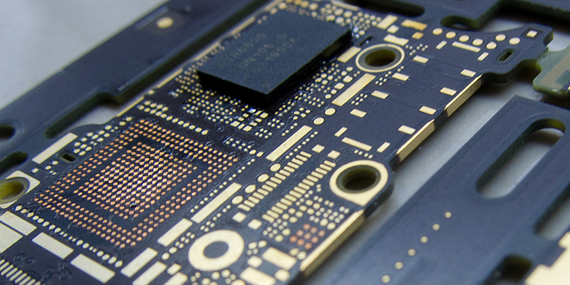
In the industry of printed circuit board manufacturing, you may have heard both the terms blind via and buried via. To understand the answer,Pls continue to look the be……
read more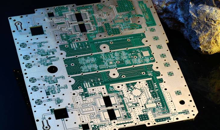
With the development of high-frequency electronic equipment, especially in wireless networks. Satellite communications are developing rapidly, and information products ……
read more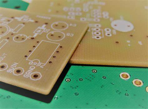
With the rapid development of the electronics industry, high Tg materials are widely used in computers, communication equipment, precision instruments and so on. in the……
read more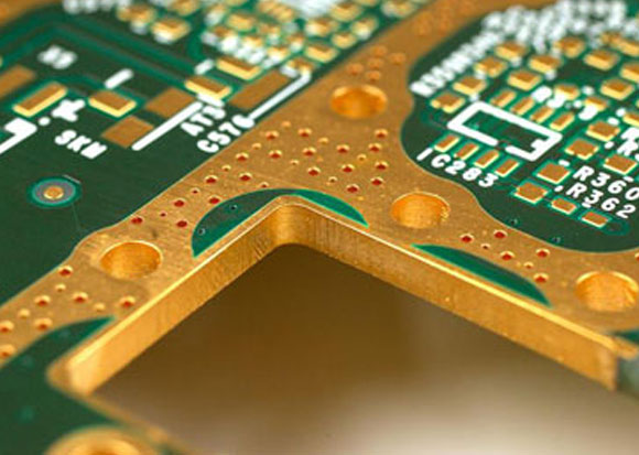
OSP is a process for the surface treatment of electronic circuit board (PCB), copper foil in keeping with the requirements of ROHS. OSP is the abbreviated form of Organ……
read more
Multilayer PCB design recommendations and examples (4, 6, 8, 10, and 12-layer boards) explain PCB design requirements. 1. Layer, Layer Is the complete ground plane(shi……
read more
Most electronics engineers encounter more or less problems when PCB circuit board prototyping design. Here I have sorted out the 10th difficult points of PCB circuit bo……
read more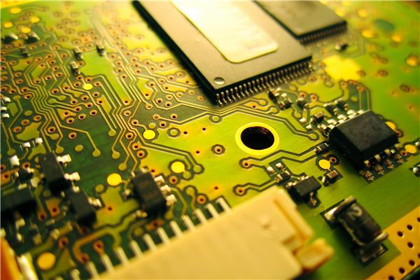
If High-speed PCB layout design can be as simple as connecting the schematic nodes and as beautiful as seen on a computer monitor, that would be a wonderful thing. Actu……
read more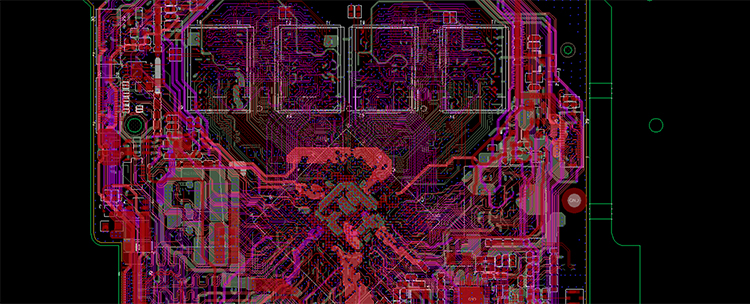
In PCB design, The design rules are the key to the success of PCB design. The intent of all PCB designers and the functional manifestations are driven and implemented ……
read more