Printed Circuit Boards
 Surface


FYPCB: Your Best Partner for Electronic Product Development.
One-stop Service for Schematic Diagram Design, PCB Design&Layout, PCB Fabrication, PCB Assembly

 PCB Assembly
 Layer Buildup
 Online Tools
 PCB Design-Aid & Layout
 Mechanics
 SMD-Stencils
 Quality
 Drills & Throughplating
 Factory & Certificate
HDI PCBs, or High-Density Interconnect Printed Circuit Boards, are advanced types of circuit boards designed to support higher circuit densities than traditional PCBs. They use finer traces, smaller vias, and stacked or buried vias to maximize the available space, allowing more components to fit into a compact area. HDI PCB technology incorporates these innovations, enhancing the performance and functionality of devices by improving signal integrity and reducing the overall size. This technology is essential for modern electronics, such as smartphones, wearables, and medical devices, where space is limited, and high-speed data transmission is required.
HDI PCBs provide a variety of advantages, making them ideal for modern electronic designs. These advantages include a smaller footprint, improved electrical performance, enhanced reliability, and cost efficiency in mass production. HDI technology allows for denser circuitry and optimized routing, which leads to faster data transmission and reduced signal interference. The compact size and high density also enable the development of smaller, lighter devices without compromising on functionality, which is particularly valuable for applications in mobile devices, wearables, and other portable electronics.
Compact Size |
Improved Performance |
Increased Reliability |
Cost Efficiency |
HDI PCBs are used in a wide range of high-performance applications due to their ability to support dense circuitry and provide superior electrical performance. These applications span across various industries, including consumer electronics, medical devices, automotive, 5G and IoT technologies, and aerospace and defense. HDI PCBs play a crucial role in enhancing the functionality, reliability, and miniaturization of electronic products, making them an essential component in today's technological advancements.
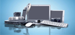
Smart phones & Consumer Electronics |
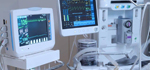
Medical Devices |
Automotive Electronics |
5G & IoT Devices |
Aerospace & Defense |
Designing High-Density Interconnect (HDI) PCBs requires a strategic approach to ensure the highest levels of functionality, manufacturability, and performance. One of the primary design principles is density and size optimization. As HDI PCBs are intended to fit more components into a smaller area, the layout must be efficient, with an emphasis on maximizing space utilization without sacrificing signal integrity. Designers also focus on signal integrity by ensuring that traces are short, direct, and free from interference. Fine traces, buried vias, and microvias are used to maintain the integrity of high-speed signals and minimize potential signal degradation.
Another important consideration is thermal management, as the increased density of components can lead to heat buildup, affecting the overall performance and reliability of the PCB. Designers incorporate thermal vias, copper pours, and sometimes heat sinks to ensure effective heat dissipation and prevent overheating. Via stacking is another common approach used to increase routing flexibility, allowing for better space management. However, this can also introduce challenges in terms of manufacturing complexity and cost. Additionally, component placement and routing must be carefully planned to ensure a balanced design that can support the necessary electrical and thermal requirements while avoiding over-complication that may affect the board’s manufacturability.
HDI PCB materials and manufacturing processes are essential to the development of high-performance, compact, and reliable circuit boards used in modern electronics. The careful selection of materials such as copper-clad laminates, flexible substrates, and advanced prepregs ensures that HDI PCBs can meet the increasing demands for smaller, faster, and more efficient devices. However, the production of HDI PCBs presents several challenges, including precision drilling for microvias, maintaining layer alignment, and ensuring thermal management. The high complexity of the design and manufacturing processes can lead to increased production time and costs. Despite these challenges, the use of advanced technology, such as laser drilling, copper plating, and effective via filling techniques, has allowed for continued innovation in HDI PCB manufacturing, making it an indispensable technology in industries such as telecommunications, medical devices, and automotive electronics. By overcoming these production hurdles, HDI PCBs continue to push the boundaries of what is possible in modern electronics, offering enhanced performance and reliability for increasingly complex applications.
| Material | Description | Technical Parameter |
Copper-Clad Laminates (CCL) | The primary base material for HDI PCBs. It is a sheet of fiberglass reinforced resin with copper foil laminated on both sides, acting as the conductor. | Copper Thickness: Typically 1oz to 3oz per ft²; Impedance Control: ≤ 5% variation; Thermal Conductivity: 0.5-0.8 W/mK (depending on type). |
Prepregs | A resin-impregnated fabric used to bond layers in multi-layer PCBs. Prepreg is partially cured to maintain flexibility during the layer-lamination process. | Glass Content: 30-40%; Dk (Dielectric Constant): 3.0-4.5; Thickness: Varies between 0.05mm-0.25mm. |
Flexible Substrates | Used in flexible HDI PCBs for bending and compact designs, typically made of materials like polyimide. | Thermal Resistance: 200°C or higher; Flexibility: Bending radius ≥ 5mm; Dielectric Constant: 3.0-4.0 (depends on material). |
Solder Mask | A protective layer applied to the PCB surface to prevent solder bridges and protect traces. Typically green, it insulates the PCB except where components are attached. | Thickness: 0.02mm - 0.05mm; Curing Temperature: 120-150°C; Dielectric Strength: 30kV/mm. |
Surface Finishes | Used to protect exposed copper pads and provide better solderability. HASL (Hot Air Solder Leveling) is commonly used, or ENIG (Electroless Nickel Immersion Gold) for higher-end applications. | HASL: Copper thickness varies, typically 1oz-2oz; ENIG: Nickel thickness: 3-6μm, Gold thickness: 0.05-0.15μm; Solderability: 24 hours shelf life |
Dielectric Materials | Used for insulating between the copper layers. Common materials include FR4 and advanced options like Teflon for high-frequency PCBs. | FR4 Dk (Dielectric Constant): 4.0-4.5; Teflon Dk: 2.1-2.3; Glass Transition Temperature (Tg): 130-180°C (depending on type). |
Microvia Fill Materials | Specialized materials used to fill microvias and buried vias, such as high-performance copper or conductive polymers. | Copper Fill: Typically ≥ 100% of via diameter; Conductivity: High conductivity copper, ≥ 100% fill for smaller vias. |
The production of HDI PCBs comes with several challenges, primarily due to their high-density design and the complexity of manufacturing processes. These challenges include the difficulty in achieving precise microvia placement, maintaining high-quality signal integrity, and ensuring efficient thermal management. The small size of components and fine traces require advanced manufacturing techniques, which can increase production costs. Additionally, HDI PCBs are more susceptible to defects like via misalignment and electrical shorts, making quality control even more crucial. Overcoming these challenges demands specialized equipment, skilled labor, and rigorous testing to ensure the reliability and performance of the final product.