
 Printed Circuit Boards
 Surface
 PCB Assembly
 Layer Buildup
 Online Tools
 PCB Design-Aid & Layout
 Mechanics
 SMD-Stencils
 Quality
 Drills & Throughplating
 Factory & Certificate


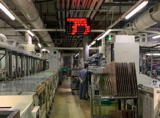
Outer Layer Etching
Outer layer etching is a crucial process in PCB manufacturing where unwanted copper is removed from the outer layers of the board to reveal the desired circuit patterns. This is typically done using chemical solutions that etch away the excess copper whil
Defines circuit patterns.
Uses chemicals for precise etching.
Ensures precision.
Minimizes waste.
Works for various designs.
Share:
-->