Printed Circuit Boards
 Surface
 PCB Assembly
 Layer Buildup
 Online Tools
 PCB Design-Aid & Layout
 Mechanics
 SMD-Stencils
 Quality
 Drills & Throughplating
 Factory & Certificate


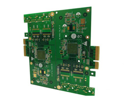
dual-thickness copper PCB
Our Dual-Thickness Copper PCB features precision-engineered layers with varying copper weights (e.g., 1oz/2oz) in a single board, ideal for high-power and high-frequency applications. Manufactured using advanced multi-layer lamination, laser drilling, and
Welcome your inquiry
Manufacturing Process: The key technical aspects of the manufacturing process are as follows: material cutting, dry film lamination, graphic transfer for the second and fifth layers, graphic etching, dry film stripping, graphic inspection, dry film lamination, graphic transfer for the third and fourth layers, graphic etching, dry film stripping, graphic inspection, browning, stacking, lamination, mechanical drilling, electrical testing, dry film lamination, graphic transfer for the first and sixth layers, graphic electroplating, graphic etching, graphic inspection, green solder mask application, silkscreen printing, shaping, electrical testing, surface treatment, final inspection, and packaging.
This process overcomes the deficiencies of existing technologies and provides a method for producing dual-thickness copper PCBs with different thickness copper foil layers in the lamination process.
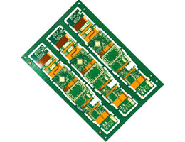
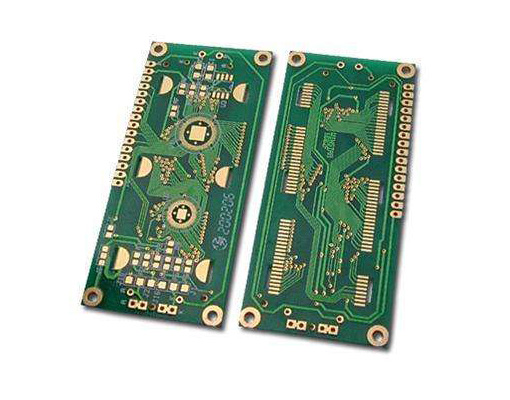
Related Products
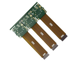
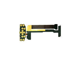
This 4-layer hybrid rigid-flex PCB combines the best of rigid and flexible circuit technologies, enabling breakthrough designs for modern consumer electronics. Perfect for applications where space constraints, reliability, and innovative form factors are