
 Printed Circuit Boards
 Surface
 PCB Assembly
 Layer Buildup
 Online Tools
 PCB Design-Aid & Layout
 Mechanics
 SMD-Stencils
 Quality
 Drills & Throughplating
 Factory & Certificate


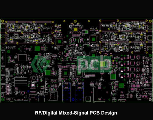
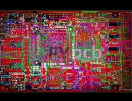
8 Layers High Frequency RF PCB Design Service China
Allegro RF/Digital Mixed-Signal PCB Design Layout
Layers: 8 layers
PIN Number: 7,000+
Board Dimensions: 250 × 180 mm
Minimum Aperture: 8 MIL
Minimum Trace Width: 4 MIL
PCB Designing Software: Allegro, Altium, Pads
Design Delivery Time: 14 days
Design Challenges: RF signal interference mitigation
Maximum Frequency: 10 GHz
Welcome your inquiry
We will provide you with quality service and guarantee
Accelerate your RF/mixed-signal projects with our Allegro-optimized 8-layer PCB design for high-frequency applications up to 10GHz. Specializing in RF/digital mixed-signal layouts, we deliver:
✔ EMI/EMC-Reduced Designs – Minimized crosstalk & optimized signal integrity
✔Allegro,Altium,Pads PCB Design – Precision routing for RF traces, power planes & high-speed digital
✔14-Day Fast-Turn Service – From schematic to production-ready Gerber files
✔ China Cost Advantage – Competitive pricing without compromising quality
Get a Free Consultation for your RF PCB project today and leverage our RF PCB design layout proficiency!
Related Products
welcome to our product consultation,here we provide you professional solutions.