Printed Circuit Boards
 Surface
 PCB Assembly
 Layer Buildup
 Online Tools
 PCB Design-Aid & Layout
 Mechanics
 SMD-Stencils
 Quality
 Drills & Throughplating
 Factory & Certificate


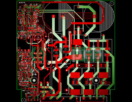
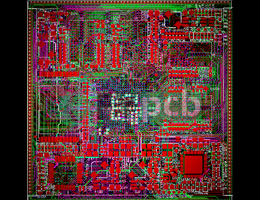
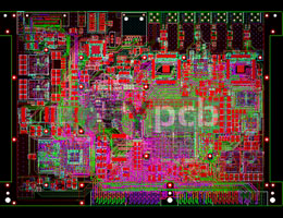
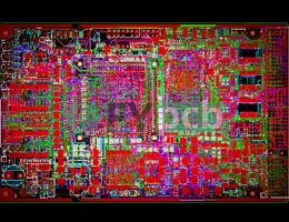
12 Layer High Density FPGA PCB Layout Design
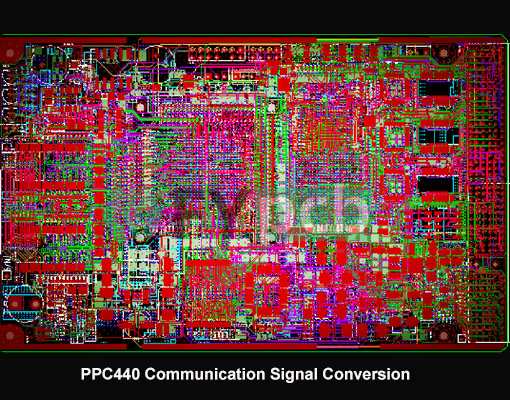
PPC440 Communication Signal Conversion PCB Design
Welcome your inquiry
FANY PCB Design Company specializes in custom PCB board design for advanced communication systems. Our 12-layer 3U CPCI PCB delivers exceptional performance for PPC440 communication PCB design with:
✔ 1.2Gb/s Signal Conversion - Optimized for high-speed data transmission
✔ High-Density Layout - 5,227 pins in compact 3U form factor (100×160mm)
✔ 10A Power Architecture - Robust power delivery for PPC440, Xilinx V3 & TI DSP
✔ Full Interface Support - 3U CompactPCI standard & RJ45 connectivity
Why Choose Our Printed Circuit Board PCB Design Service in China?
Allegro/Altium/PADS Experts - 9-day guaranteed design delivery
High-Density Solutions - 4mil traces, 0.20mm microvias, and EMI control
End-to-End Custom PCB Board Design - From concept to production-ready files
Request Design Files or Get a Free Quote for your PPC440 project today!